on
Using the ARM cores on the Xilinx Zynq 7000
In this post we will build on our first experience with the Xilinx tools and learn how to use the ARM cores to interact with the programmable logic. This is the second post in the Zynq 7000 seminar series; in this post I will show how to achieve communication between the programmable logic (PL) and processing system (PS) sides of the Zynq 7000.
The other posts in this series are:
- Getting started with the Xilinx Zynq 7000
- Using the ARM cores on the Xilinx Zynq 7000 [This Post]
- Zynq 7000: Using a Command Line Workflow
- Zynq 7000: Adding Custom Blocks
In this example we will control the LEDs on the Red Pitaya board, which are connected to the FPGA, using the ARM microcontroller. This can be accomplished entirely using the free IP cores provided by Xilinx alongside the Vivado IDE, so we will not be using any custom RTL code in this post.
Block Design
For this post we will once again use the graphical tools to create a block design, as in the previous post. Use the same steps as before to create a project called “axi-gpio” (again targeting the “xc7z010clg400-1”) and a block design called “axi_gpio”. Like in the previous example, we will first add the “ZYNQ7 Processing System”. Once the block has been added it will show in the block design. The “Run Block Automation” should now be available; use this to add the two external interfaces (DDR and FIXED_IO) to the block design. The result should look something like the image below.
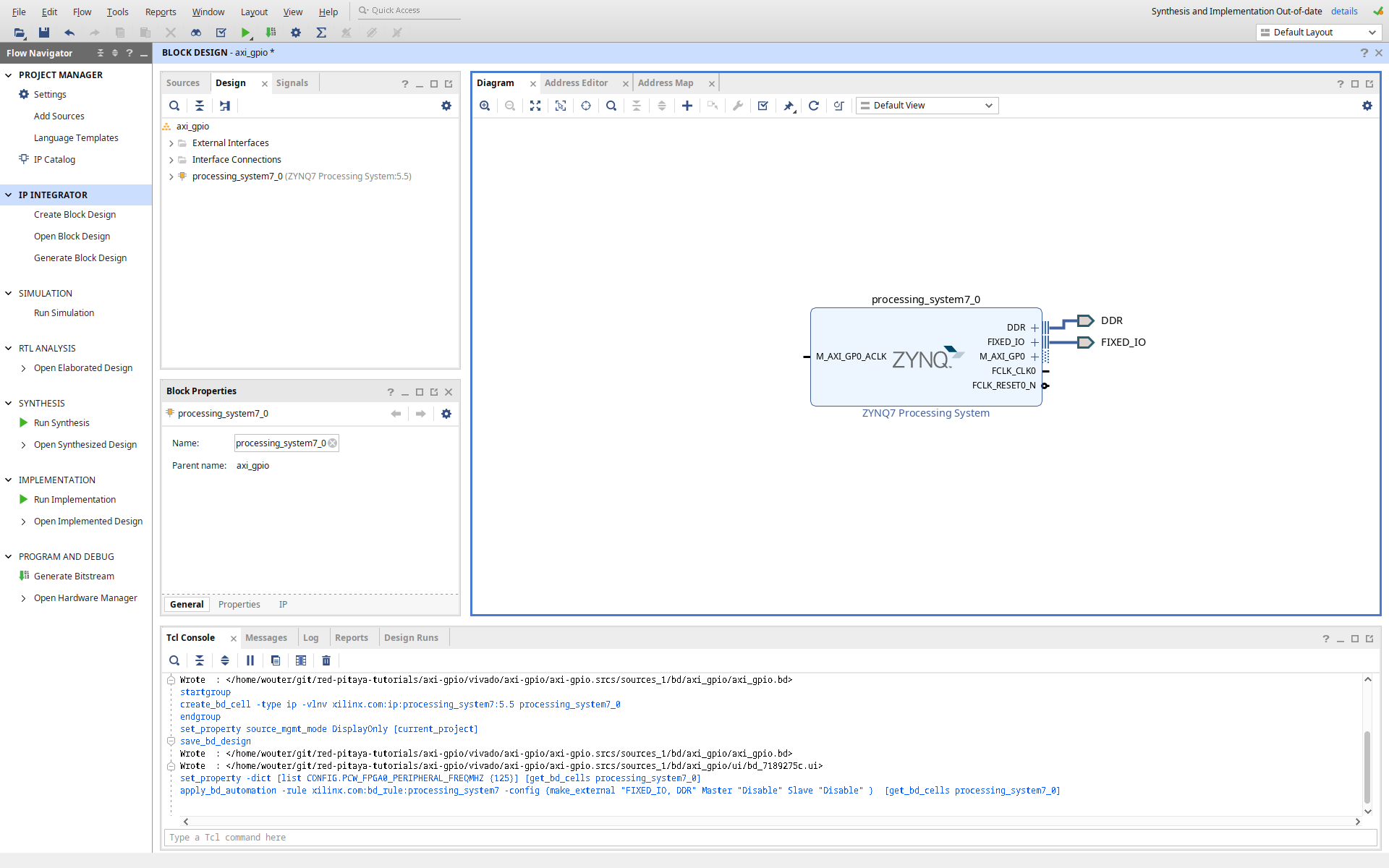
Like in the previous post, Vivado will have to know what the clock frequency of the FCLK_CLK0 clock will be.
Double click on the “ZYNQ7 Processing System” and use the “Clock Configuration” tab to configure the fabric clocks.
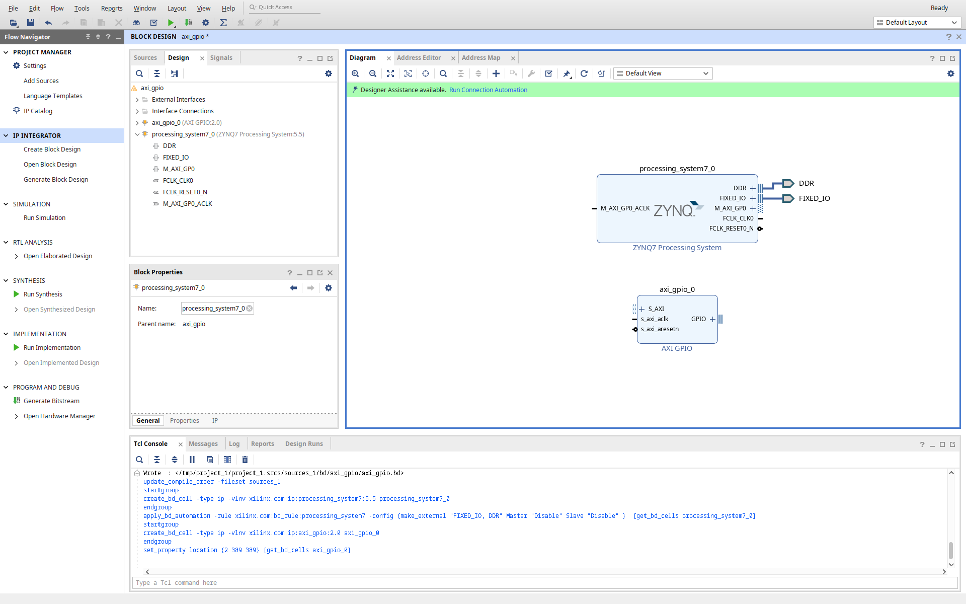
To control the LEDs on the Red Pitaya we have to add another block to our design: the AXI GPIO block. We can add this using the “Add IP” button, just as with the Zynq 7 Processing System. You should see a new block in your block design, similar to my result below.
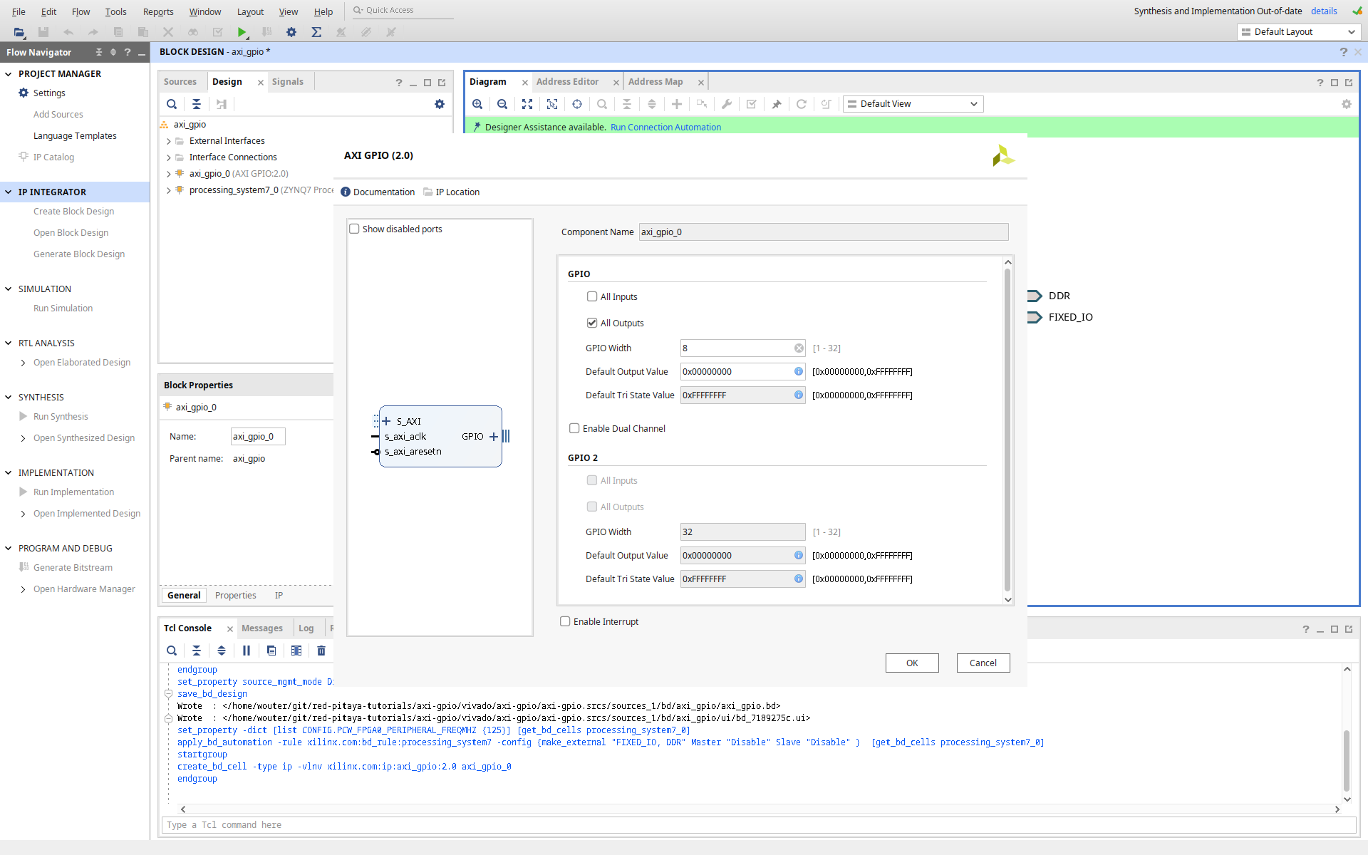
This block will also require some configuration. The AXI GPIO block provided by Xilinx is quite generic; it can be configured with up to two independent channels, which can each be configured with up to 32 I/O lines per channel. Each channel can be configured to be bidirectional IO, input only or output only. As before, the configuration options can be brought up by double clicking on the AXI GPIO block. Change the GPIO width to 8 to match the 8 LEDs, and enable the “All Outputs” mode. The configuration should now match the one shown below.
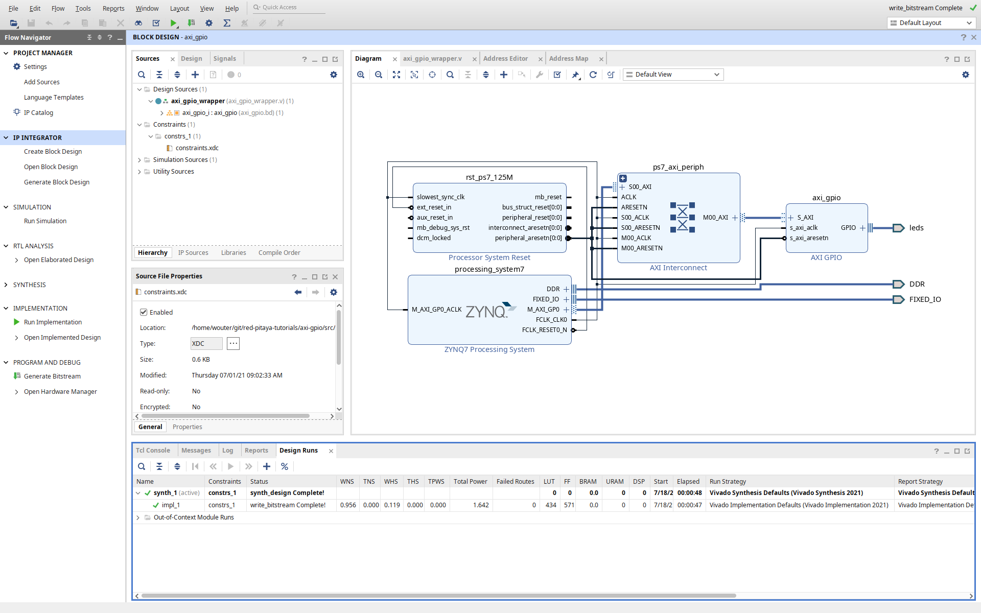
Now we have to connect the AXI GPIO block to the ZYNQ7 Processing System so that the ARM cores can write to the registers in the block and configure the GPIO pins. Another green bar should have shown up at the top of the screen, this time offering to run connection automation. Click on the link to open the connection automation dialog; in the pane on the left you should see all items which can be automatically connected. In this case we will choose to connect both items: the GPIO interface, which will be external, and the S_AXI interface which will connect to the ZYNQ7 Processing System (we can leave all the S_AXI options at their defaults). The diagram should now contain the same blocks as in the image below; the location of the blocks may vary depending on where you placed the first two blocks. If you want to get the same layout as below you can use the “Regenerate Layout” option by right clicking on the block design, or by pressing the circular arrow button on the toolbar.
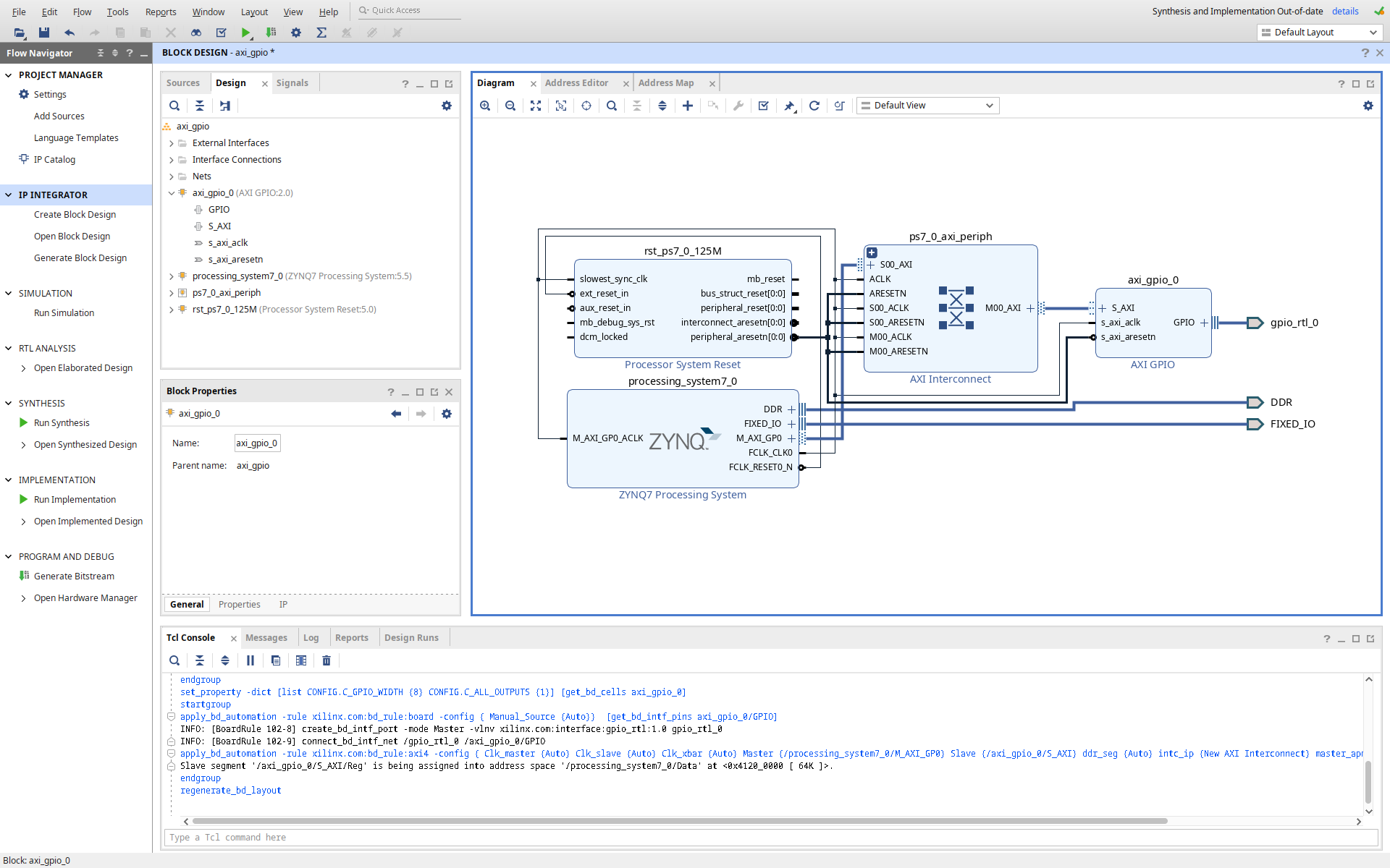
Before I explain the blocks that have been added in the previous step I am going to rename the port gpio_rtl_0 to something that is more descriptive and easier to understand. Since this port will drive the LEDs I have named it leds. You can change the name in the “External Interface Properties” window (to the left of the block design) after clicking on the external port.
In this step the design automation has added two new blocks to the block design: the “Processor Reset System” and the “AXI Interconnect”. The reset system takes all the reset sources and combines them and synchronizes them into a clock domain. I am planning to explain why this is necessary in a future post, so for now I will just say that this block is necessary to get reliable reset behaviour. The interconnect allows us to connect multiple blocks to one AXI interface on the Processing System. In this example we only have block so we do not strictly need the interconnect, but Vivado adds it anyway to make it easier to add more blocks later on.
As a side note, the interface name “S_AXI” identifies this as an AXI slave interface. I will not go into too much detail about the AXI protocol today, because that will be the topic of the next post. For now, however, it is useful to know that the AXI interface is memory mapped. This means that the registers in this block can be accessed by writing to or reading from specific addresses in the memory space of the PS. The base address for each AXI slave interface is configured in the address editor in Vivado (which we will cover later); the offset for each register is defined in the RTL inside the IP block. Memory-mapped access is a very convenient method for controlling peripherals, and this is found in many embedded platforms.
Because the peripheral will be memory mapped, we have to configure its address range.
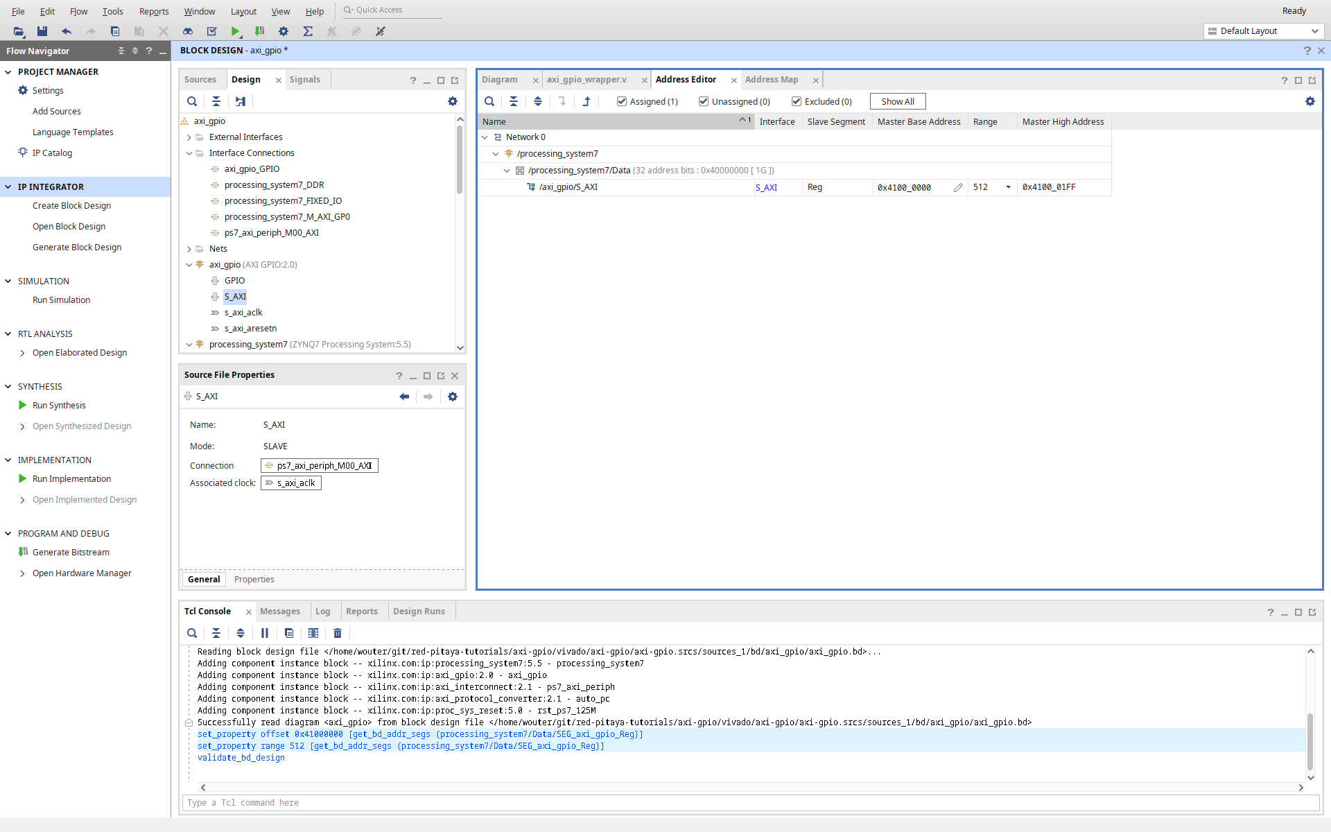
To do this open the “Address Editor” tab on the top of the screen; this should look like the screenshot below.
This screen shows all the AXI networks in the design and the AXI slaves which are connected to these networks.
Each slave can be configured with a base address and a range using this interface.
In this design there is only one network, with a single slave: the AXI GPIO block.
I have configured the block to have a base address of 0x4100_0000; you can use a different address but you will need to adjust the subsequent code examples to match.
The range should be chosen to cover all the valid addresses inside the block; in this case this is 512 bytes (you can figure this out from the Product Guide for the core, or from the number of address bits on the AXI interface).
A larger range is also valid, but inefficient as there will be wasted address space.
The block design is now complete, and we can add the wrapper. In the sources pane, right click on the block design and create the HDL wrapper and let Vivado automatically manage it. Next we have to add the constraints to the project. As we discussed previously, constraints are a way to specify additional information about your design to the toolchain. Use the same steps as in the previous post to create a new constraints file and add the following lines:
|
|
This constraints file is a bit different from the one used in the previous post.
The single bit led signal has now been replaced with a bus (a signal containing multiple bits) named leds_tri_o.
The wildcard [*] is used to select all the bits in the leds_tri_o bus so that the properties are applied to all the bits in the bus.
The leds_tri_o bus corresponds to the leds port in the block design.
The leds port is a special type of port, called an interface port, which can contain multiple signals and therefore Vivado mangles the signal names.
In this case the suffix _tri_o is added the end the of the port name; the _o is because we selected the outputs only option in the IP block configuration.
In lines 5-12 a physical pin is assigned to each bit in the leds_tri_o bus.
In previous post I discussed the various ways in which you can figure out which pins to use, but I will briefly list them again here:
- Using Red Pitaya’s default constraints file.
- Using the Red Pitaya’s partial schematic.
- Using Red Pitaya’s online documentation.
The final step is to generate the bitstream, which can be done by following the same steps as in the previous post. Start the process by clicking on “Generate Bitstream” in the “Program and Debug” section. If Vivado asks whether it is OK to run synthesis and implementation first, click Yes. Before moving on, use the Design Runs tab to confirm whether the timing requirements have been met.
Processing System
The PL bitstream is now finished and ready to use, and the next step is to write some software to control the AXI GPIO module from the ARM cores.
We could do this using a baremetal program (so without the Linux OS), or we could use the devicetree in the Linux kernel to register the AXI GPIO block and use Xilinx' kernel driver, or we can use mmap and /dev/mem to control the registers in the AXI GPIO module directly.
In this post we will write a simple C program which will run in Linux userspace using the latter approach.
The other two approaches will be covered in future posts.
/dev/mem is a special file which gives access to the physical memory space, which is very convenient for accessing I/O registers for peripherals.
Of course it also has large security implications, as it gives you access to all the memory of the system…
To access /dev/mem you need to have both the regular file access permissions and the security capability CAP_SYS_RAWIO, or you can execute the program as the root user.
To keep things simple we will use the root user for now, and we will discuss the other options in a future post.
In order to ascertain what values need to written to the registers in the AXI GPIO core, we can read its documentation (“AXI GPIO v2.0 Product Guide”, PG144). The register space for the AXI GPIO core is described on page 10 of the product guide, and I have included a screenshot of this page below.
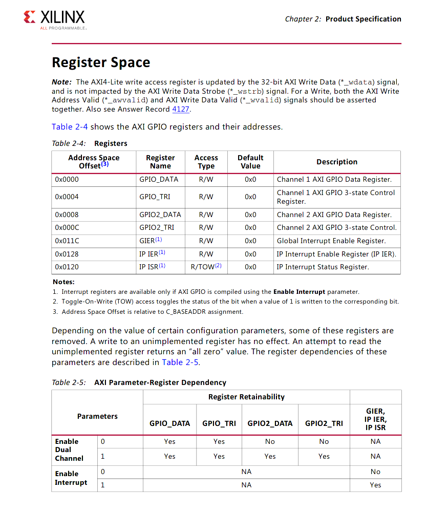
The register space is shown in Table 2-4; some other interesting information can be found in Table 2-5, which shows which registers are actually available based on the configuration parameters of the core.
Since we did not enable the second GPIO channel or the interrupts, we only have pay attention to the first two registers, GPIO_DATA and GPIO_TRI.
The latter controls the direction of the GPIO pins, allowing them to be configured as inputs or outputs.
Since we configured the core as outputs only, we can ignore the GPIO_TRI register.
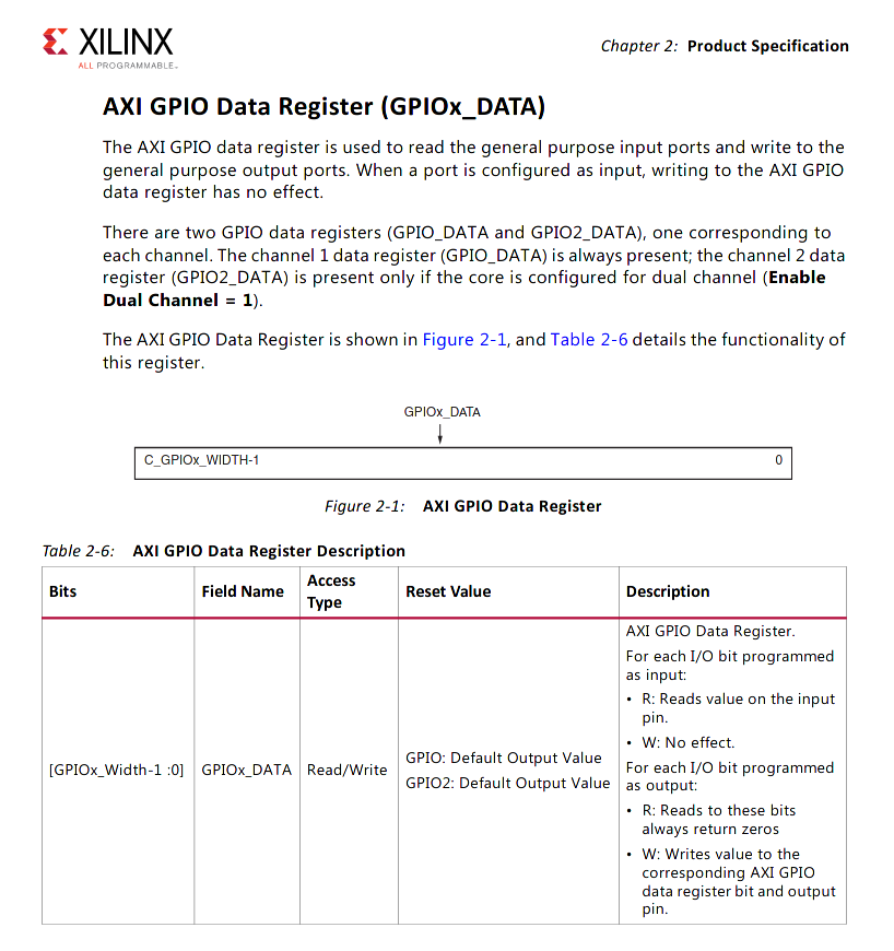
That leaves the GPIO_DATA register; an explanation about the contents of this register can be found on page 11 (which is also included below).
It can be seen that only the lower N bits of the 32-bit word are valid, where N is the number of I/Os configured for that IP core (in our case, 8).
It also shows for bits corresponding to output pins (all bits in our case) a write will write that value to the I/O pin, while a read will always return 0.
The listing below shows a C program which will toggle an LED roughly every second.
The main function performs the following steps:
- Open
/dev/memto access the system’s physical memory - Use the helper function
zynq_mapmem()to map the address space corresponding to the AXI GPIO block - Write to the register at offset
0to change the state of the IO pins
|
|
This program works by creating a file mapping using the mmap for the special ‘file’ /dev/mem.
When reading from or writing to /dev/mem offsets in the file correspond directly to byte address in the physical memory space of the system.
The mmap function allows to map a part of the /dev/mem file of a given size and offset into the virtual address space of our process.
The size and offset have to be multiples of the page size of the operating system (typically 4096 bytes).
In this case we map a single page and the offset is the address of the AXI GPIO block we configured in the Vivado Address Editor (0x4100_0000).
The function then returns a pointer to the address in the virtual address space of the process where the file mapping has been created.
Accessing data via this pointer corresponds directly to accessing the physical memory bus at the offset we specified.
Hence p_axi_gpio[0] corresponds to the address 0x4100_0000, and p_axi_gpio[1] corresponds to the address 0x4100_0004 (note that p_axi_gpio is a uint32_t* so the physical address increases by 4).
The easiest way to compile simple programs like this is to copy the code onto the Red Pitaya and compile it there.
In a future blog post I will explain how to configure a cross-compilation environment which would allow you to compile the executables directly on your development machine.
So, you can use scp, WinSCP, FileZilla or something similar to copy the code onto your Red Pitaya, and copy the bitstream at the same time:
Next log into Red Pitaya using the serial console or using SSH. Once you have connected to the Red Pitaya you can run the following command to compile the program:
Finally program the PL with the bitstream and run the C program:
You should see that the LED only blinks when the blink_led program is running, as shown in the animation below.
An Additional Example
The code below demonstrates an example with a slightly more interesting pattern. This is one of the advantages of using an SoC like the Xilinx Zynq: the code running on the ARM cores can be modified and iterated upon much faster than the HDL that defines the PL bitstream.
|
|
Fundamentally this code is the same as the previous example and the interaction with the PL is done in the same way: it uses mmap to access the registers in the AXI GPIO IP block and the zynq_mapmem helper function has remained unchanged.
The only changes are in the main function, where the pattern to be displayed on the LEDs is calculated.
The new program can be copied to the Red Pitaya and compiled in the same way as the previous code; I used the following commands on my Red Pitaya.
After running this program, you should see the following pattern on the LEDs.
Summary
In this post we have learnt how to use a key feature of the Zynq-7000 SoC: the processing system. We have seen how IP cores can use AXI4 interfaces to connect to the processing system, and how they can be mapped into the address space of the processor. In this example we then used a C program and memory mapping to access the registers in the IP core.