on
Getting started with the Xilinx Zynq 7000
The Xilinx Zynq 7000 series systems-on-chip (SoC) combine an FPGA with ARM Cortex-A9 microprocessor cores, providing buses for transferring data between the two parts of the SoC. These devices are excellent for data acquisition tasks: the FPGA can be used to interface with high-speed data convertors such as ADCs and DACs, and to apply computationally intensive data processing tasks to the data. The processed, and potentially downsampled, data can then be transferred to the ARM core(s) for further processing.
Since the ARM cores are normal microprocessors they can be programmed using standard software tools, which most developers are already familiar with. The ARM cores can execute code without an operating system (baremetal mode) or they can run Linux; the dual-core variants can also run Linux on one core only. Running Linux has some advantages: you get a fully-featured networking stack, filesystem drivers, USB drivers (for a USB WiFi dongle, for example) and plenty of libraries which already work on Linux. You could even attach a screen, keyboard and mouse to a Zynq SoC to get a standard Linux desktop experience.
This post will be the first in a series on the topic of how use the Zynq SoC for data acquisition projects. The series is loosely based on a number of seminars which I have presented to the research group over the years. And whilst the series will focus on Zynq SoCs, much of what will be discussed can be applied to other Xilinx 7-series FPGAs or even FPGAs from other manufacturers. The Zynq 7000 series currently contains the following posts:
- Getting started with the Xilinx Zynq 7000 [This Post]
- Using the ARM cores on the Xilinx Zynq 7000
- Zynq 7000: Using a Command Line Workflow
- Zynq 7000: Adding Custom Blocks
I have chosen to use the Red Pitaya STEMLab 125-14 as the development board for this series of posts. With two 125 MSPS 14-bit ADCs and two 125 MSPS 14-bit DACs, it is a very powerful data acquisition platform. My colleagues and I have used this device for as the basis for multiple different electromagnetic sensors: for a handheld metal detector, to detect buried iron meteorites and for novel measurement equipment.
In this first post I will demonstrate how to put together a simple Zynq 7000 project using Xilinx Vivado (which is included with the Xilinx Vitis toolchain) and the Linux SD card image provided by Red Pitaya. In this example we will blink an LED on the Red Pitaya at a rate of approximately 1 Hz using the FPGA fabric. We will do this by connecting the most significant bit of a binary counter to the LED.
FPGA Block Design
In this example we will use a Block Design (BD), which is a Xilinx Vivado feature where all the elements of the design are presented as blocks which can be wired together. The end results looks a little like the schematic representation of a circuit. When I first got started I found that this approach gave me a nice overview of what my FPGA design was doing, and it helped reinforce the point about the inherent parallelism in FPGAs. The block designs are also an easy way to instantiate and configure the vendor IP cores, including the ones provided by Xilinx inside Vivado.
Block designs are not the only method which can be used; it is possible to select a HDL source file to be implemented instead. In fact, behind the scenes this is how the block designs work: Vivado generates a file which implements the block design in VHDL or Verilog and it is this file which gets used for the synthesis.
Before we can get started the Xilinx Vivado toolchain has to be installed. This can be either be installed on its own or as part of the Xilinx Vitis suite; I recommend the latter option because I will be using Vitis in future posts. Beware, however, that FGPA toolchains are very large: the version of Vitis currently installed on my laptop (2021.1) takes up 81 GB of disk space.
Once installed, launch the Xilinx Vivado IDE and create a new project. This will launch the project wizard, where you can select the project name, location, type, design sources and the FPGA type you are targeting. I have named the project “rp-blink-led”, but you could choose a different name. For this project we want the “RTL Project” type, we do not have to add any design sources or constraints at this stage, and we are targeting the “xc7z010clg400-1” part.
This is the part number for the specific Zynq 7000 series SoC found on the Red Pitaya STEMLab 125-14; the “xc7” refers to the Xilinx 7 series of devices; the “z” identifies that it is a Zynq device; the “010” is the model number, which determines the specification such as the amount of logic gates, block RAM etcetera; the “clg400” refers to the package of the device, in this case a 0.8 mm pitch grid array package with 400 pins; and finally the “-1” refers to the speed grade, which has an impact on the maximum achievable speed of the FPGA fabric and other elements inside the FPGA.
Once the project has been created, it should open automatically to the Project Manager view. On the left hand side there is a pane called the “Flow Navigator”, which allows the user to switch between a number of views (or flows as Xilinx calls them). You can click on the name of the view to switch to it, or you can click on the links underneath to perform related actions.
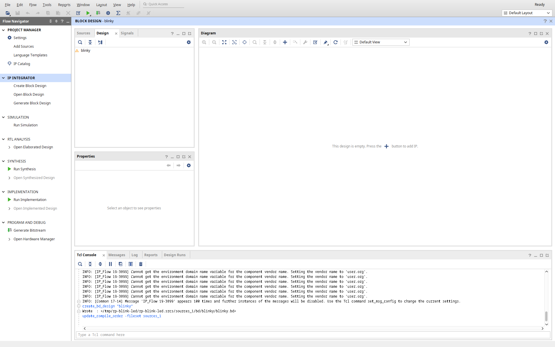
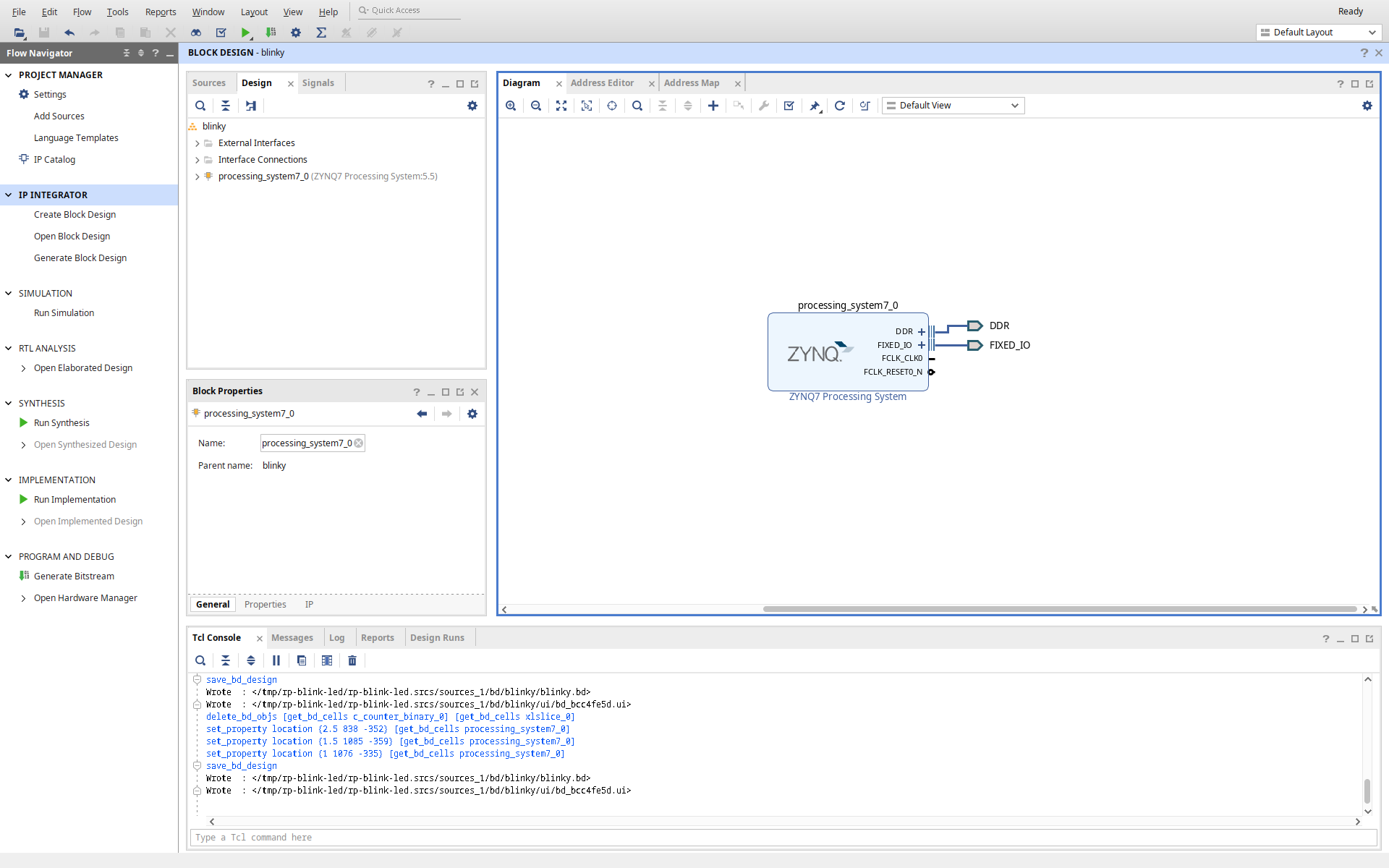
Under the IP Integrator view you can create a new block design; I chose to name the design “blinky”, though this is not important for the rest of the tutorial. After the block design has been added, it should open automatically and your screen should look something like the screenshot below.
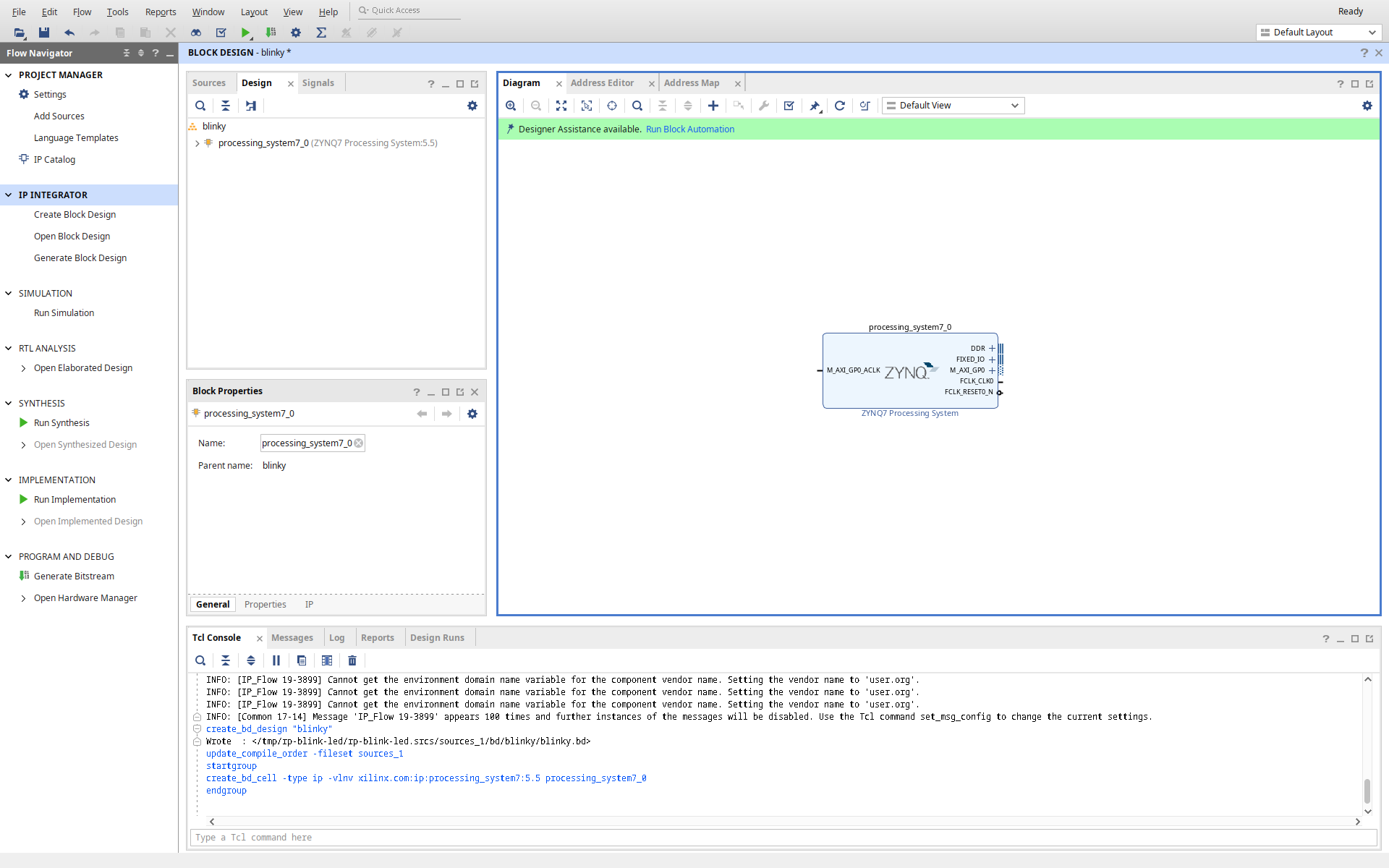
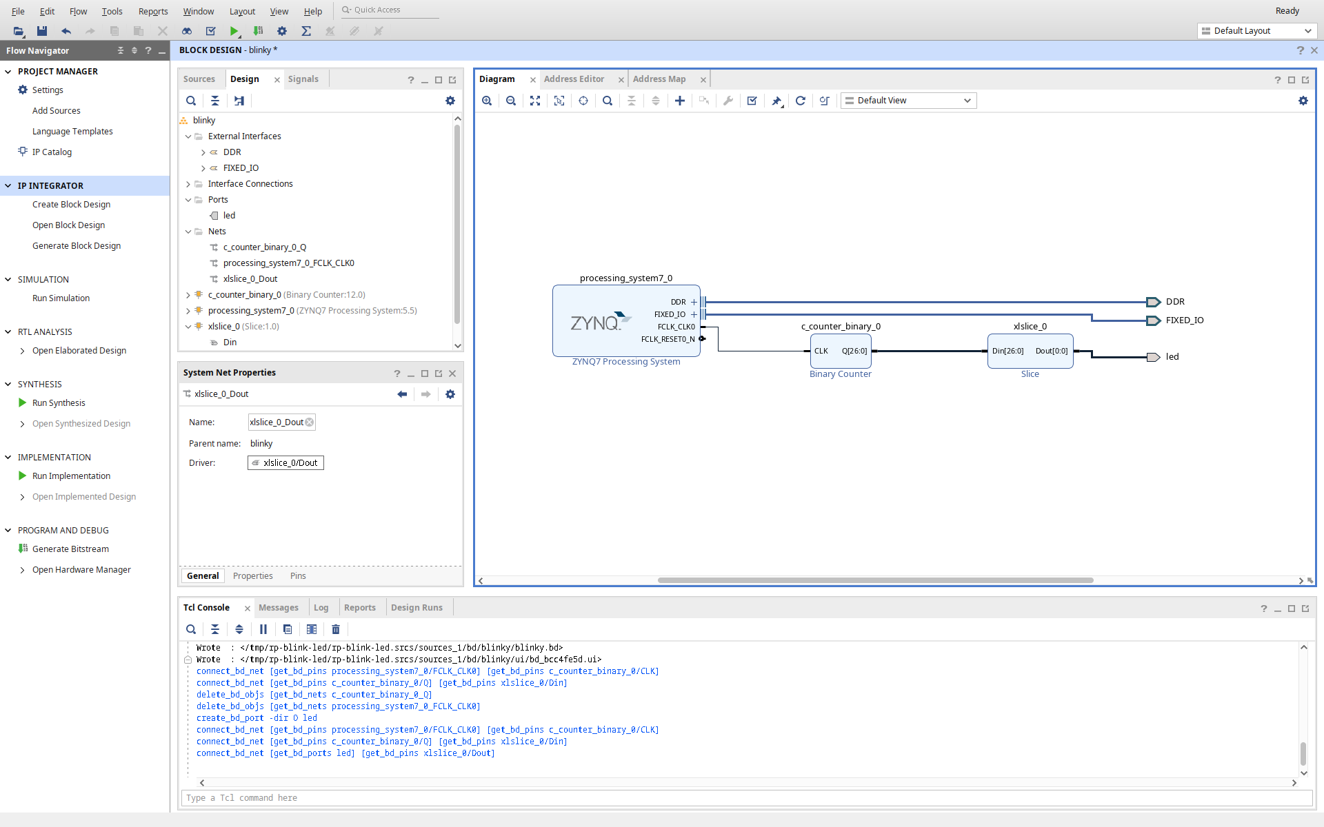
We can now start adding blocks to add functionality to our design. The first block to add will be the “ZYNQ7 Processing System”, which acts as a wrapper around the interface between the FPGA, also called the Programmable Logic (PL) and the ARM microprocessor cores, also called the Processing System (PS). This interface gives access to up to 4 clock signals which are configured by the PS, and their associated reset signals (more on this later); multiple general-purpose and high-performance AXI busses for transferring data between the PS and PL (more on these in the next post); and a host of other configuration options.
Blocks can be added either by pressing the ‘+’ button in the toolbar, using the keyboard shortcut ‘CTRL+I’ or by right clicking and clicking on “Add IP…”. This will bring up a context menu showing all the available IP cores. Select the “ZYNQ7 Processing System” by scrolling down or by typing part of its name. Once the block has been added it will show in the block design, which should now look similar to the following screenshot.
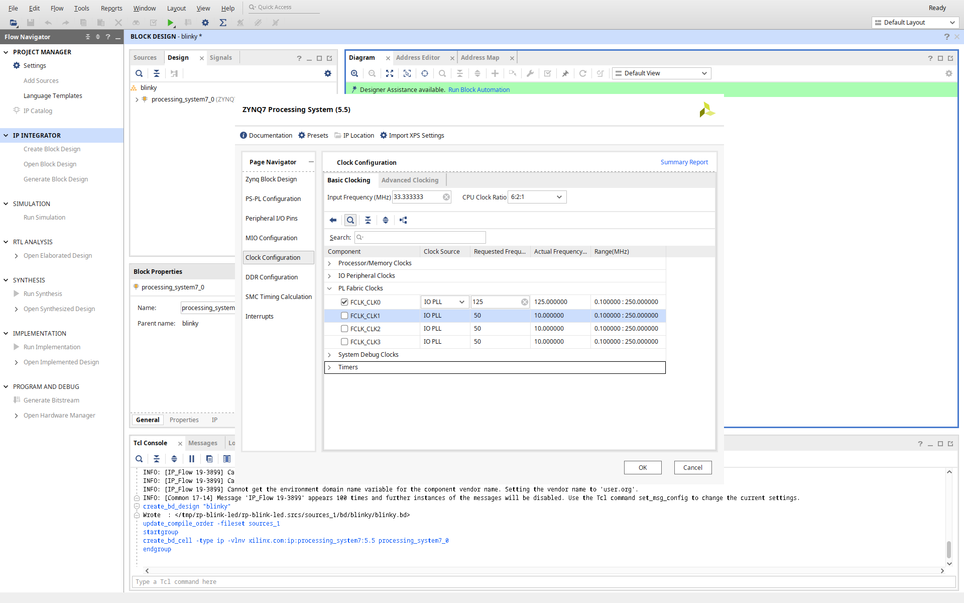
All IP blocks can be configured by double clicking on them, or by right clicking the block and selecting “Customize Block” in the context menu. Some blocks present a very simple dialog, while others have very elaborate options. The Zynq 7 block has a lot of configuration options and has a nice looking dialog. For this project we only have to configure the clock speed of the clock signal “FCLK_CLK0”. So in the Zynq 7 settings go to the “Clock Configuration” tab, and expand the “PL Fabric Clocks” section. In this section make sure that “FCLK_CLK0” is enabled and set the frequency to 125 MHz.
At this point I should note that these clock frequencies are not controlled by the PL; they are controlled by the PS and changing the value in this dialog does not actually the change the clock frequency. The clock frequencies here are purely informative: Vivado has to know the clock speed so that it can properly synthesize a bitstream to program the PL. There is no way for Vivado to determine what frequency the PS will configure for these clocks, so you have to use this dialog to tell Vivado the clock frequencies.
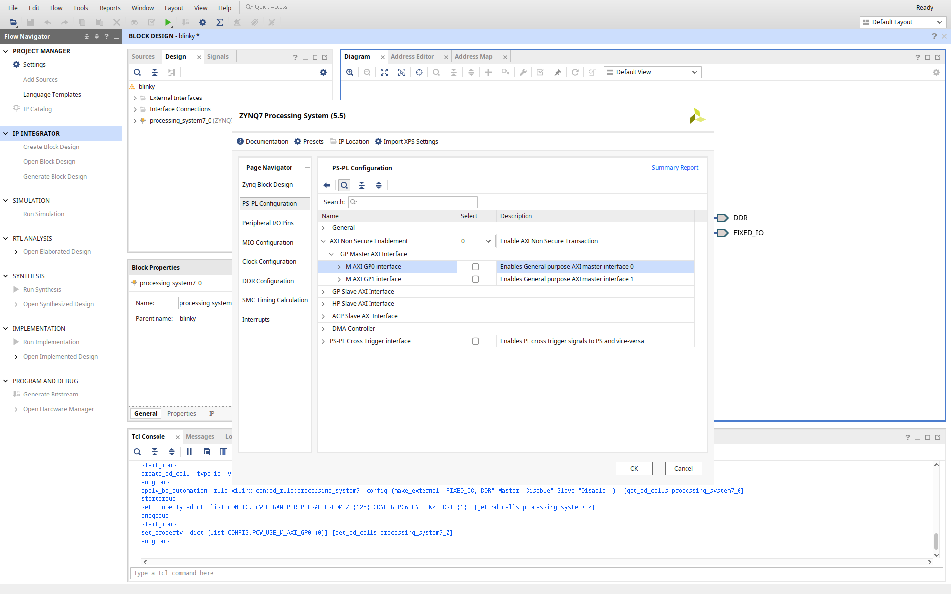
The other change to make is to disable the M_AXI_GP0 interface. You can skip this step and leave the interface disconnected, but I thought I’d show this step for the sake of completeness.
In the configuration screen for the Zynq 7000 block open the “PS-PL Configuration” tab, and expand the “AXI Non Secure Enablement” item and then the “GP Master AXI interface”.
Then make sure the tickbox for the “M AXI GPO Interface” is disabled.
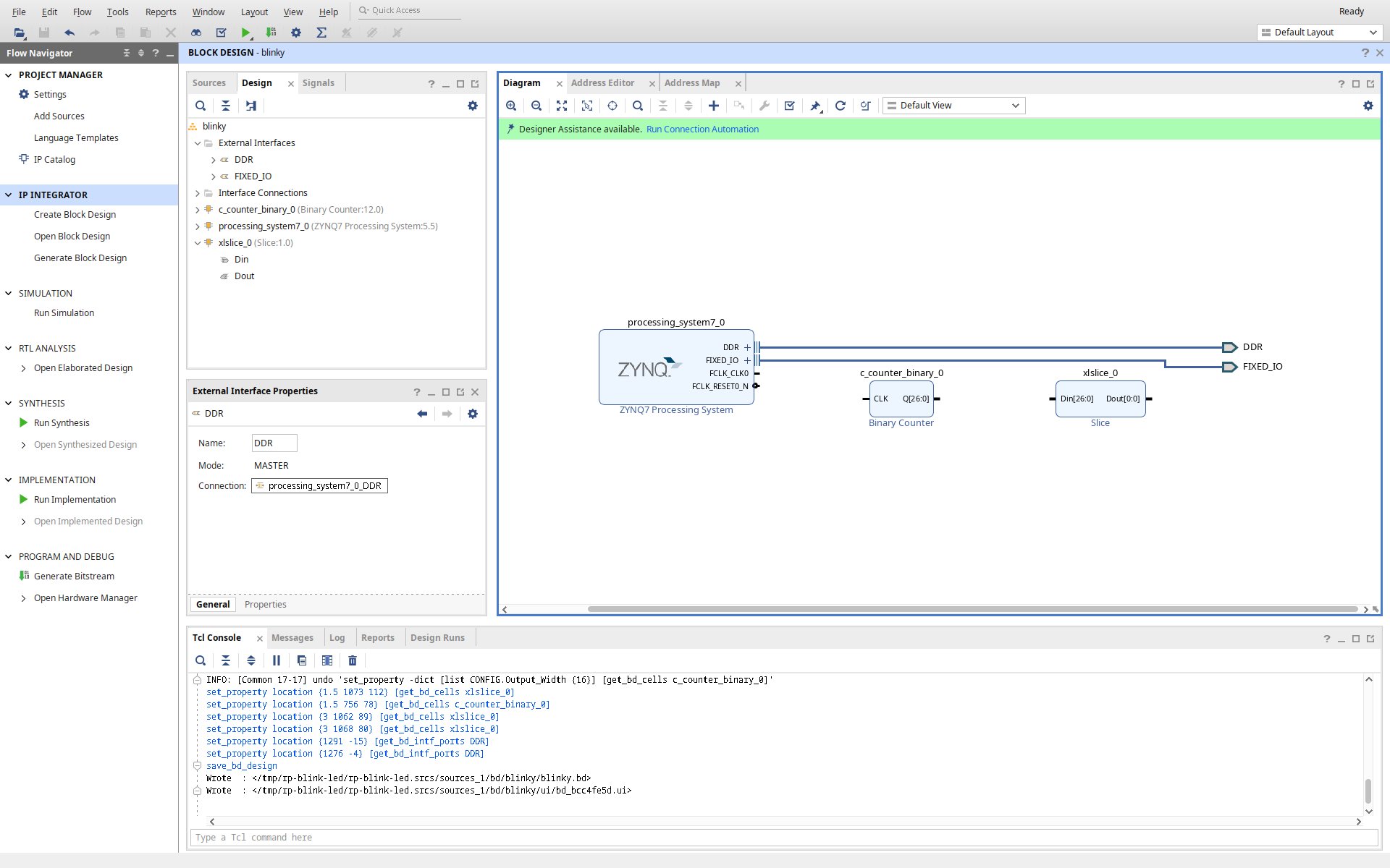
Next we will connect up some of the external interfaces of the ZYNQ7 processing system. Vivado offers some nice assistance in wiring up certain blocks, in the form of either block or design automation. Whenever these automated rules can be applied a green bar appears on the top with a link to open up the relevant dialog. Click on “Run Block Automation” now, and use the default settings. This will add two external interfaces (DDR and FIXED_IO) to the block design and connect them to the Zynq 7 PS block. The result should look something like the image below.
To drive the LED signal we have to add two more IP blocks: a “Binary Counter” block and a “Slice” blocks. We can add these using the “Add IP” button, just as with the Zynq 7 Processing System. The tool adds the blocks in arbitrary locations, but I prefer to lay them out as follows.
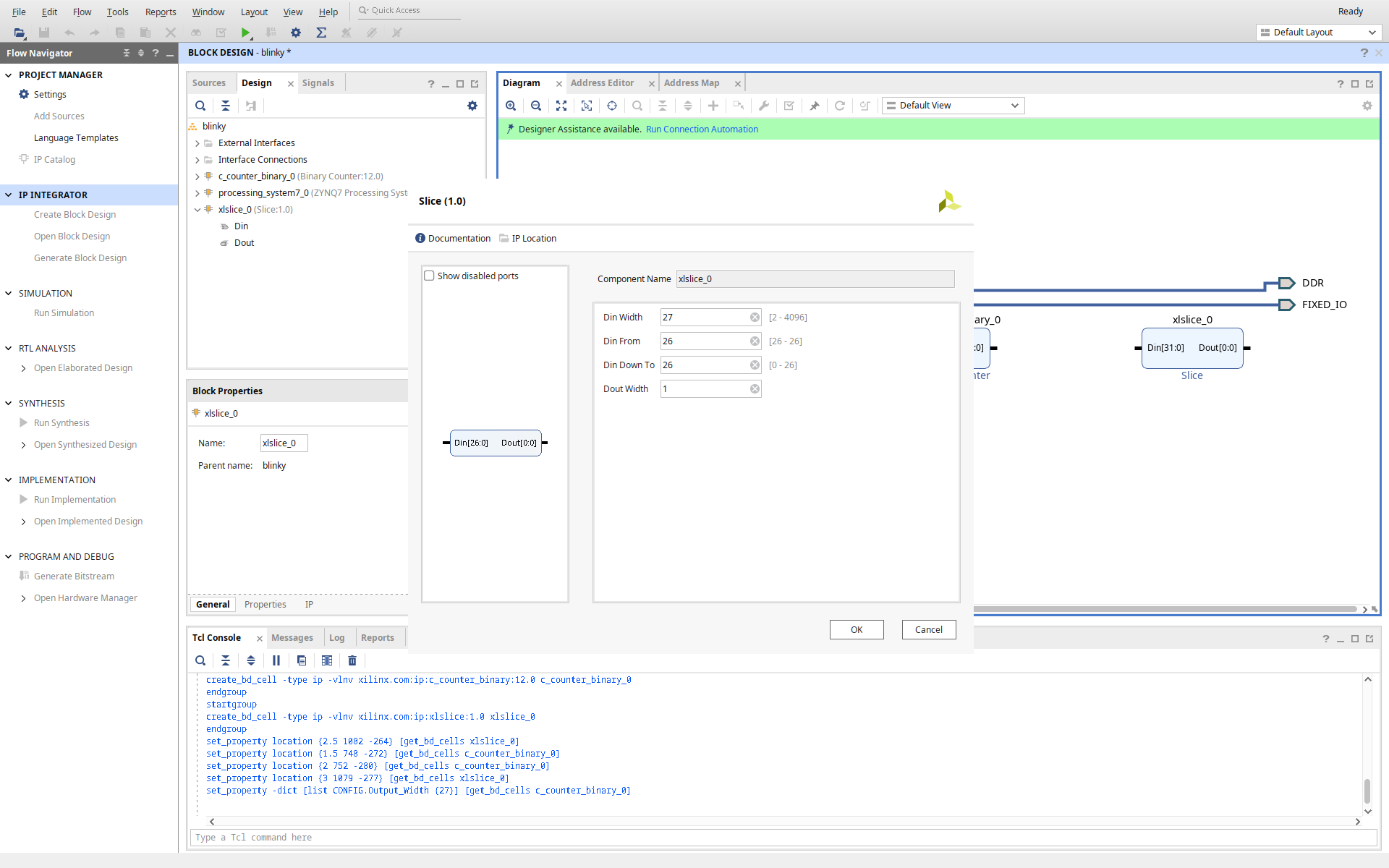
These blocks will also require some configuration. The first step is to change the width of the binary counter; open the counter configuration by double clicking on the IP block. On the settings page, change the output width to 27, which gives us a rate of approximately 0.93 Hz (125,000,000 / 2^27 = ~0.9313 ). Next we have to configure the slice block to select the most significant bit of the 27 bit signal. Double click on the slice block and change it to match the follow configuration.
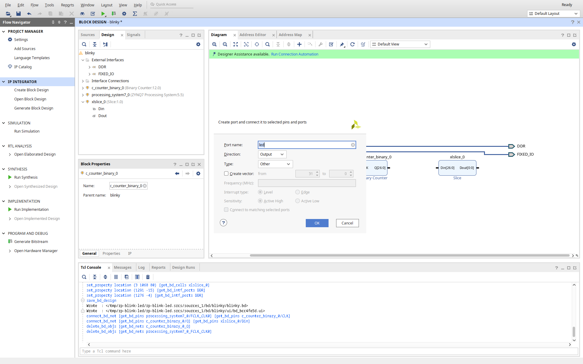
The output from the slice block will be what drives the LED on the board. In order to make this connection we have to expose the signal to the outside of this module using a port. You can add a port by right clicking on the block design and choosing the “Create Port” option in the context menu, or by using the “CTRL + K” keyboard shortcut. This should show a dialog like in the image below. In this dialog, name the port “led” and set the direction as “Output”.
All the elements in the design have now been added and configured, and all that remains is to connect them together. Connect the FCLK_CLK0 pin on the “ZYNQ7 Processing System” to the “CLK” input on the binary counter, connect the output from the binary counter to the input of the slice block and finally connect the output from the slice block the “led” port. The final result should look similar to the image below.
From Block Design to Bitstream
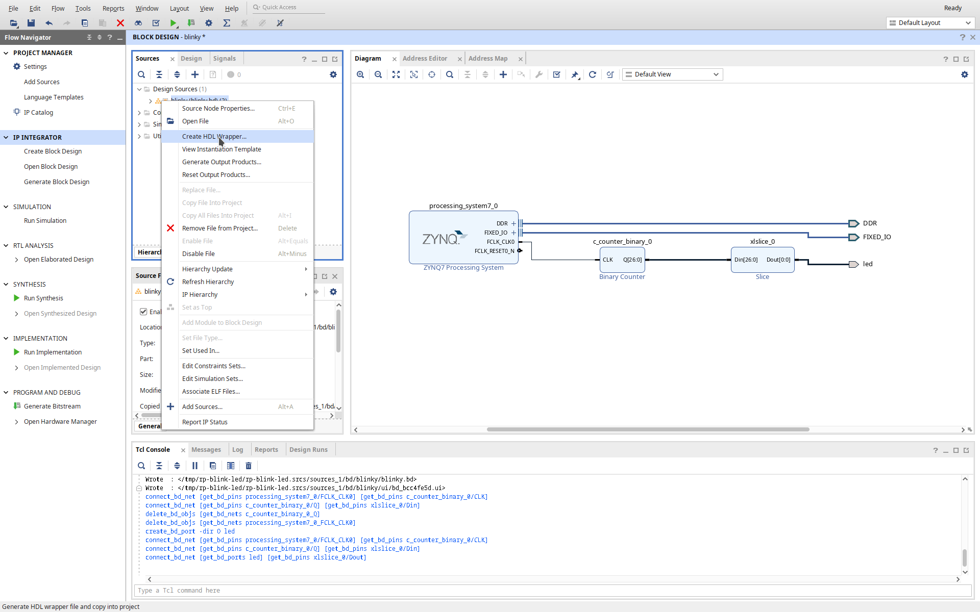
The block design is now complete. For Vivado to be able to synthesize this design, a VHDL or Verilog file has to be wrapped around the block design. Vivado can automatically create and manage this wrapper, which is very convenient for simple designs. In the “Sources” tab near the top left of the screen, right click on your block design and then click on the “Create HDL Wrapper” option. In the dialog that appears, choose to let Vivado automatically manage the wrapper.
Next we have to add some constraints to the project. Constraints are a way to specify additional information about your design to the toolchain. You can specify timing information, which pins to use for external signals, which physical standards to use for each pin, and debugging information, amongst other things. Some constraints are automatically added by the IP blocks, but others have to be added by the designer. For this project we have to use constraints to specify some information about the pins connected to the LEDs. Use the “+” button in the sources tab (top left) or the keyboard shortcut “Alt + A” to add a new source file, select the option to “add or create constraints” and add a file named “constraints.xdc”. Open the new file (you can find it in the “Constraints” folder) and add the following lines:
In line 1 we specify the I/O standard as 3.3V LVCMOS, which you can read more about on Wikipedia. In line 2 we specify the slow slew rate; the slew rate refers to the rise and fall times of signal, and controlling these is important for maintaining signal integrity and EMC compliance. For LEDs we do not care about the rise or fall time, so we can use the slow rate. In line 3 we set the drive level to 8, which means that the maximum current at which the 3.3V LVCMOS specifications can be met is 8 mA. In line 5 the led signal is connected to the physical pin F16.
There are a few ways in which you can work out which pins to connect the signals to. The first is by reading the constraints file used in the default Red Pitaya firmware, which you can access here. The second option is to review the schematics of the Red Pitaya board; while the full schematics are not available, you can access a partial schematic which contains enough detail for most projects. Finally, if you are wanting to connect your signals to the extension connectors, their pinout is also listed in the Red Pitaya documentation.
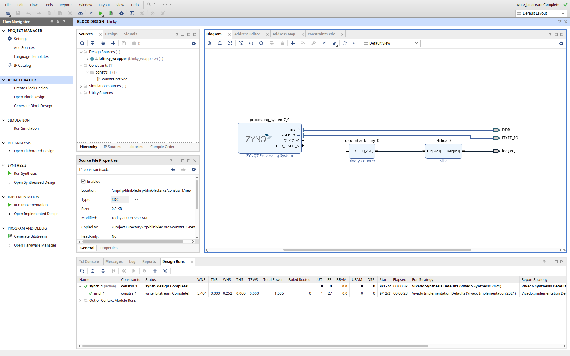
In order to program the FPGA in the SoC a bitstream has to be generated. To get the bitstream, click on “Generate Bitstream” in the “Flow Navigator” pane, under the “Program and Debug” section. If Vivado asks whether it is OK to run synthesis and implementation first, click Yes. After some time a dialog will appear to confirm that the process has finished and the bitstream has been written.
When the bitstream has successfully been generated it is important to confirm that the timing requirements have been met. If the requirements are not met, some parts of your design might not be capable of running at the specified operating frequency. Unfortunately Vivado does not make it very clear when the timing is not met, so this has to be checked manually. The easiest way to check is to open the “Design Runs” tab at the bottom of the screen and check that WNS (worst negative slack) and WHS (worst hold slack) are both positive, and that TNS (total negative slack) and THS (total hold slack) are both zero and that TPWS (total pulse width slack) is zero. The meaning of each of these numbers will be discussed in a future post.
Loading the Bitstream
I will describe two methods for loading the bitstream onto the PL on the Red Pitaya.
The first uses an external JTAG programmer, which can do more than just programming as it also allows access for debugging.
If there is a Linux operating system running on the ARM cores, as in the default Red Pitaya image, it is possible to use this to program the PL.
This functionality can be accessed via a special file in the /dev/ folder.
First I will describe how to use the Linux OS to load the bitstream onto the PL. This method is nice because it does not require any additional hardware, which is great if you do not own a JTAG programmer or are out on the road without access to one. It does, however, remove the ability to use some of the debugging tools inside Vivado.
Connect the power supply and ethernet to the Red Pitaya. The ethernet cable can be connected via a network (using a router or switch) or as a peer-to-peer connection between the Red Pitaya and the host PC. Optionally you can also connect the Red Pitaya’s serial console to the PC.
Next we have to make sure that we can log into the Red Pitaya via SSH, and that we can make file transfers to it.
If your development machine uses Linux this can done using the command line tools ssh and scp respectively.
On Windows I normally use PuTTy and either WinSCP or FileZilla.
You will have to make sure your development machine has one of these tools, or an equivalent tool, installed.
The default SD card image supplied with the Red Pitaya assigns a hostname to each device based on its MAC address.
The address should be written on a sticker on top of the ethernet jack and should have the format RP-xxxxxx.local.
If your host supports mDNS, you will be able to connect to the Red Pitaya using this hostname.
Use ssh or PuTTy to verify that you can connect to the Red Pitaya, by opening an SSH session (the default login details are root:root).
If you cannot connect to the Red Pitaya using the hostname on the sticker, you can log in via the serial console and run the command ip a to find the IP address of the Red Pitaya.
You can then use this IP address to open an SSH session instead of the hostname.
Once you have successfully connected to the Red Pitaya, we will copy the bitstream to the Red Pitaya.
On the development PC, locate the bitstream that was generated by Vivado.
In my case the path looks something like this:
/home/wouter/xilinx/rp-blink-led/rp-blink-led.runs/impl_1/blinky_wrapper.bit
Of course the project location will be different on your computer, and if you used different names for the project and/or block design, you will have to account for that as well.
Using the file transfer program of your choice, and using the same host or IP address and login details from before, transfer the .bit file to the Red Pitaya (for quick prototyping I normally place the file in /root on the Red Pitaya).
The screencapture below shows the process from a Linux based host, using ssh and scp.
The bitstream can then be loaded onto the FPGA by running the following command on the Red Pitaya:
|
|
Summary
In this first post we have learnt how to use Vivado to create a block design, how to add blocks to the design and how to generate a bitstream from it. We also learnt how to use SSH and SCP to copy files to the Red Pitaya and how load the bitstream onto the programmable logic in the Zynq SoC. In this post we only used the PL section of the Zynq SoC, without using the ARM cores (PS). The next post in this series will show how to use the PS to interact with the PL.