on
Zynq 7000: Adding Custom Blocks
In the previous posts we have build our designs using just the built-in IP blocks provided by Xilinx inside Vivado. At some point you will likely want to add more specialized behaviour using bespoke HDL code. In this blog post I will explain how to add custom modules to a Vivado block design. The functionality in this design will mirror that of this previous post, where we made an LED blink at a constant rate. In this example we will replace the Xilinx' binary counter and slice IP cores with our own RTL code.
This post is part of a series on programming the Xilinx Zynq 7000:
- Getting started with the Xilinx Zynq 7000
- Using the ARM cores on the Xilinx Zynq 7000
- Zynq 7000: Using a Command Line Workflow
- Zynq 7000: Adding Custom Blocks [This Post]
RTL Code
The listing below shows the RTL code we will use to drive the LED. As I mentioned in a previous post, the aim of this series is not to teach the basics of HDL programming, but rather the specifics of using the Zynq 7000 SoCs and the Red Pitaya system in particular. Therefore I will only cover the contents of the code at a high level. The module has one parameter, controlling sets the width of the counter which is simply counts up every clock cycle until it overflows and wraps around. The output signal driving the led is the most-significant bit of the counter value. This all matches exactly with the design we used in the first post, except it is now implemented using our bespoke Verilog code as opposed to using Xilinx IP blocks.
|
|
Vivado GUI
In Vivado create a new project (I called mine blink-led-rtl) using the same steps as before.
After the new project has been created and opened, add a new source by right clicking on “Design Sources”, then “Add Sources” (or alternatively, hit ALT + A) and choose to “Add or create design sources”.
Click next, then click on “Create File”; in the dialog set the file type to “Verilog” and the file name to “blink.v”.
Click on OK and then finish to add the new file to the project; when the “Module Definition” window appears you can just click OK without making any changes.
If Vivado asks you whether you are sure that you do not want to change the module definition, click yes.
The new file should appear under “Design Sources”; open the file now and copy and paste into it the contents from above.
We can also add the following constraints to the project using the same steps from the first two posts:
Now that all the the text sources have been added, we can create the block design (I named mine “blinky_rtl”), again using the same steps as before.
In the block design, first add the “ZYNQ7 Processing System” IP block, run the block automation, disable the AXI GP0 bus and set the FCLK0 frequency to 125 MHz. This follows all the same steps from the previous post.
The next step is to add our blink HDL module to the block design.
This can be done by right clicking on the block design and choosing the “Add module…” option from the context menu.
A new window should appear showing all the available modules in the current project.
In this case we only have the blink module available, so make sure it is selected and click OK.
A new block now appears in the block design with the same interface we defined in our Verilog code (a clk and led signal).
Connect the clk pin on the blink module to the FCLK_CLK0 pin on the ZYNQ7 block and create an output port named led (either by right clicking on the block design or using the shortcut CTRL + K) and connect it to the led pin on the blink module.
The final block design should look similar to the screenshot shown below.
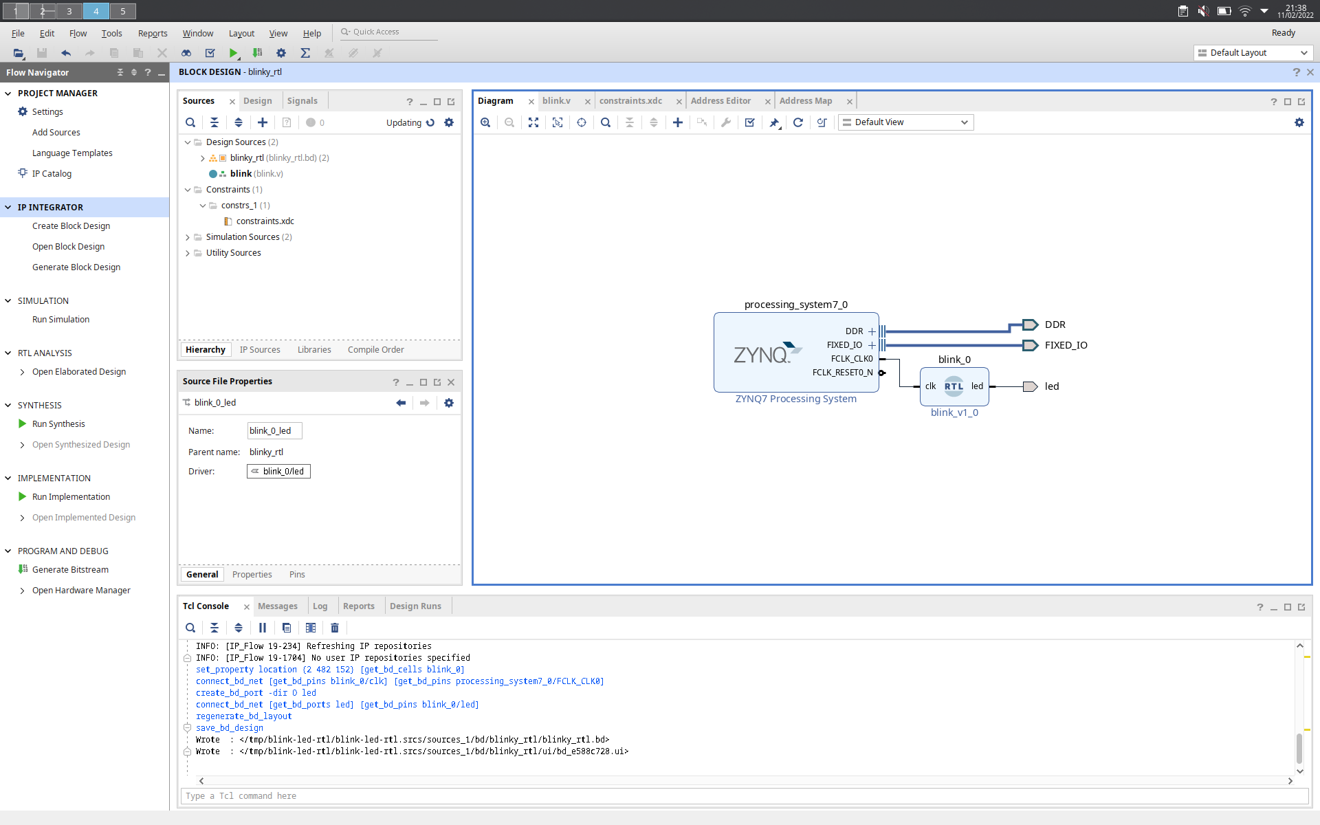
Looking at the block symbol for the blink module, you can see a logo saying “RTL” in the middle of the block.
All blocks based on RTL modules have this logo on them, allowing you to easily locate them.
Now you can create the HDL wrapper and then generate the bitstream, just as in the first blog post.
Loading the bitstream onto the FPGA should result in the LED blinking in the same way as before.
Adding a Reset
This section is not actually specific to adding bespoke logic to your designs, but it seemed like a good place to talk about it.
In general it is a good idea to add a reset signal to your logic (though there definitely valid reasons not to in certain situations).
For our blinky module, this might look something like this:
|
|
Here the reset signal is named rstn, and when asserted it resets the counter value to 0.
It is a synchronous reset (because the value rstn is considered used on rising edges of the clock signal) and active-low (because it is considered asserted when rstn is 0).
Now add these changes to the blink.v file in your project and save the file.
Vivado should now show a new bar at the top, offering to “Refresh Changed Modules”, as shown in the screenshot below:
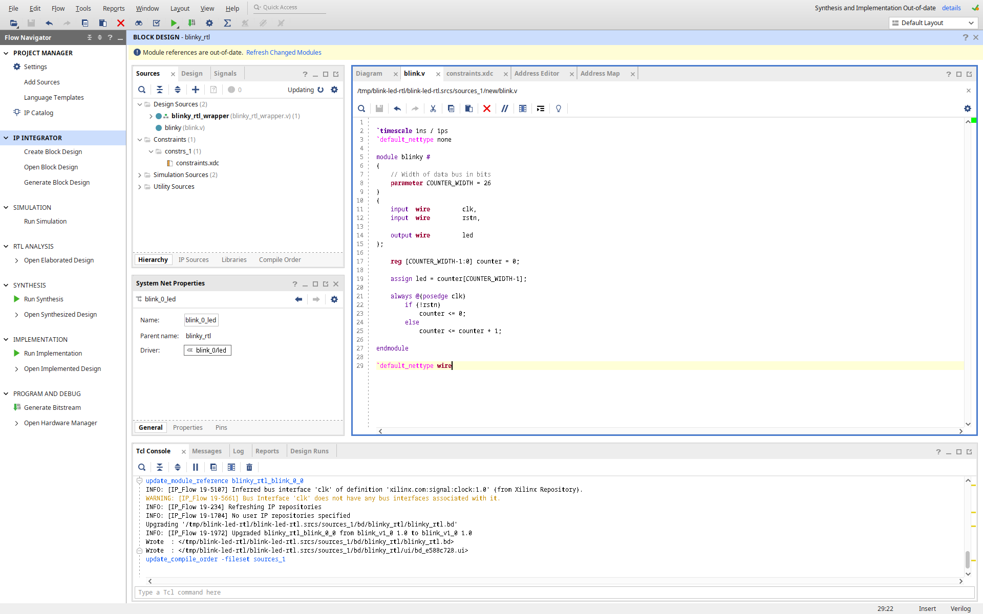
When making changes to source files that are used as, or in, modules in a block design you must click this option before re-running the synthesis and implementation process; if you do not do this, the synthesis will use the old version of the source files.
Click on this now to start the process.
At this point Vivado should take you back to the block design, and you will like get a warning similar to the one below, stating that Vivado identified potential issues when upgrading the core.
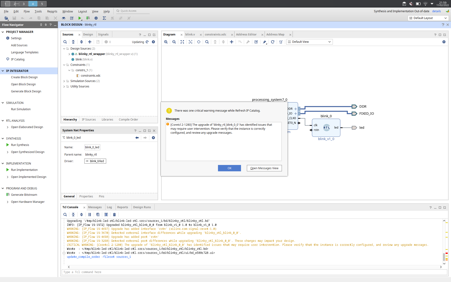
This message appears when the interface (the input/output ports and parameters of the module) has been changed.
In this case it appears because we added the rstn port, and Vivado was not able to connect it to anything automatically.
The next step is to provide a connection for this signal; unfortunately we cannot connect it to the FCLK_RESET0_N signal directly.
This is because FCLK_RESET0_N is an asynchronous reset signal (i.e. it is not synchronised to FCLK0), but our module expects a synchronous reset.
If we did connect them directly together we might run into issues with closing the timing on our project.
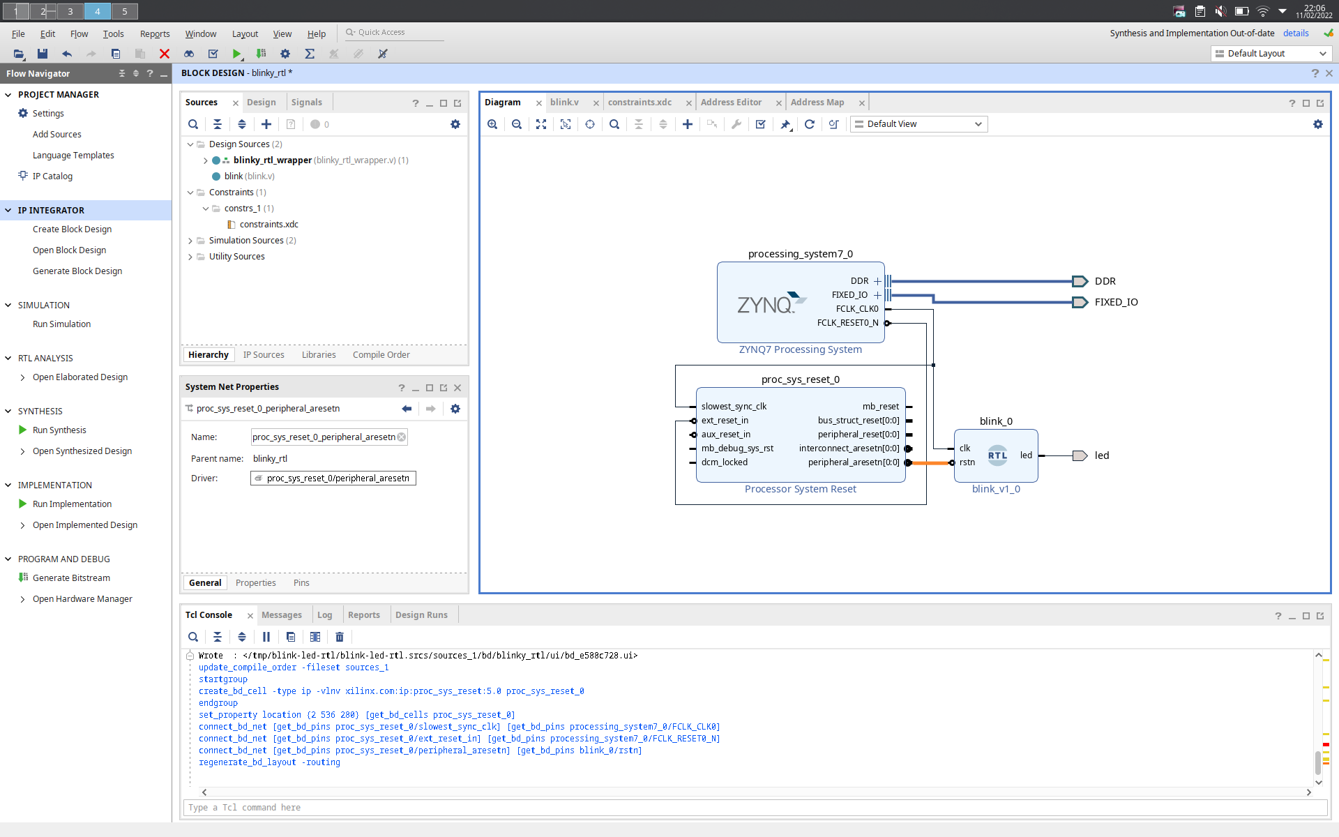
Instead we will add another IP core to the block design to synchronise the reset signal for us.
The name of the IP core is “Processor System Reset”; add this to your block design now and make the following connections:
FCLK_CLK0on the ZYNQ7 block toslowest_sync_clockon the reset blockFCLK_RESET0_Non the ZYNQ7 block toext_reset_inon the reset blockperipheral_aresetnon the reset block torstnon theblinkymodule
The end result should look similar to my block design:
You can now regenerate the bitstream and upload it to the FPGA, and the LED should blink the same way it did before. The reset signal is not particularly important in this project, but I was keen to discuss how to handle reset signals in Zynq-7000 projects as it does come up in most designs. We already came across the “Processor Reset System” in the second post of the series. In that example, however, we were able to use the design automation wizard to automatically add the reset system. In general, any time you interact you with the ZYNQ7 processing system, you will need to add a processor reset system; if your design has multiple clock domains, you may need one per clock domain. In most cases the design automation wizard will guide you though this, but it is good to know why these blocks are being added.
Command Line
Following along the theme of the previous post in the series, I will also share how to implement this project using the command line workflow.
You can view the TCL scripts and other sources on GitHub.
The project structure is the same as before, but I have added a new directory, src/rtl/, to hold all the RTL sources (the blink.v file from above).
The contents of the mk_proj.tcl file are the same as in the previous blog post, the only addition is the line
|
|
which adds the RTL source file to the project.
The TCL script to create the block design, src/bd/blinky_rtl.tcl, is shown in the listing below.
|
|
The main difference from the previous script is the following line, which shows the syntax for adding a block based on an RTL source file, as opposed to an IP core:
|
|
In the TCL command above the -reference blink refers to the module blink defined in the blink.v file. blink_0 is the name that the created cell will get in the block design.
You can use mk_proj.tcl and build.tcl in the same way as before to first create the project and then generate the bitstream.
Summary
RTL modules are a way to add bespoke behaviour to your block designs without having to go through the process of packaging up the IP (I will try to cover this process in a later post). In this post we have seen how to add a module based on custom RTL code to your Xilinx projects and block designs, using either the GUI or the command-line workflow.